Role Do Solder Masks Play in Circuit Board Assembly
When designing or troubleshooting a circuit board, the quality of your solder mask plays an important role. As such, understanding the key functions and properties of solder masks is essential for any PCB engineer.
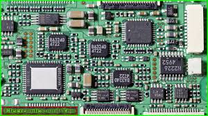
Solder masks are the protective polymer layers that cover the copper traces on a printed circuit board assembly. They shield the conductive metal from corrosion, and are available in a variety of colors. The most common color is green, but blue, black, red, purple, and clear options are also available. Choosing the best color for your PCB depends on many factors, including component placement, design requirements, and the intended product use.
A key function of solder masks is to protect the copper traces from external factors that can cause shorts or other defects. These include dust, dirt, moisture, and other contaminants that can reduce conductivity or lead to failure. They also help prevent oxidation of the copper, which can impair performance over time.
What Role Do Solder Masks Play in Circuit Board Assembly?
Another critical function of solder masks is to define the areas where solder should and should not flow. This prevents bridging between adjacent pads and traces, which can cause electrical shorts and other defects during reflow. It also ensures that the correct solder paste is applied to each pad.
Once the solder mask is applied, it must be cured to harden. This process involves exposing it to heat and UV light for a certain amount of time. The curing process varies between different types of solder mask and manufacturers. The right combination of temperature, UV exposure, and time is necessary to ensure that the solder mask will be durable and able to withstand the production and usage process.
A faulty or inadequately cured solder mask can cause several problems during assembly and use. These include solder bridging, which occurs when the solder flows between two closely spaced pads and causes an electrical short; pinholes, which are small holes in the mask that expose the underlying copper and can cause electrical shorts; and delamination, which is the separation of the solder mask and copper from each other.
The first step in circuit board assembly is the creation of the bare printed circuit board (PCB). This involves designing the circuit layout using specialized software, followed by etching the design onto a copper-clad board. The etching process removes excess copper, leaving behind the desired circuit pattern. Once the PCB is created, the assembly process can begin.
The best way to avoid these issues is to follow good practice when designing a circuit board. This includes using a solder mask that meets your specific needs, following proper application and curing processes, and testing the quality of the finished product to ensure its functionality and durability. NEXTPCB offers high-quality solder masks that meet these requirements and are backed by an experienced team of engineers and technicians. Learn more about our services and how we can help you create the perfect PCB for your next project!